SUDACNC provides full-cycle professional PCB design engineering service for global OEM & ODM electronic developers. Our experienced layout engineers complete schematic drawing, multi-layer PCB layout, high-speed differential signal routing, controlled impedance traces, power thermal dissipation design, EMC/EMI noise reduction and RF antenna layout. We conduct strict DFM manufacturability review before file delivery to avoid fabrication and assembly defects, output complete production files including Gerber, drill, BOM, CPL coordinate and assembly drawings. Compatible with rigid, flexible, rigid-flex and HDI microvia circuit boards for consumer IoT, industrial control, automotive and medical electronics. All designed PCBs can be directly transferred to our internal PCB production workshop and EMS SMT assembly lines, realizing one-stop closed-loop electronics development from design to finished box build devices.
All circuit design data secure & fully confidential NDA protection
Seamless handover to our PCB manufacturing & EMS assembly lines
What Is Professional PCB Design Engineering?
PCB Design is the core engineering link converting electronic circuit logic into physical manufacturable printed circuit board layout. It includes two core phases: schematic capture to define component connection logic, and PCB layout to arrange device placement, trace routing, power ground partitioning, thermal copper layout and shielding structures.
Amateur layout often ignores signal integrity, impedance matching, heat dissipation and EMC rules, leading to unstable prototype performance, mass production short circuits and high failure rates. Our professional PCB design strictly follows IPC industry standards, combines manufacturing process limits of our own PCB factory and SMT workshop, completes pre-production DFM optimization, and outputs fully compatible production documents. Paired with our in-house PCB fabrication and EMS assembly service, we eliminate cross-supplier communication errors, shorten product development cycles and reduce overall electronic hardware R&D costs for startups and medium-sized electronics brands.
Six Integrated Full-Lifecycle PCB Design Engineering Modules
Our PCB design workflow covers complete hardware development from circuit logic definition to factory-ready production documents, six interconnected engineering modules eliminating information gaps between design and manufacturing. Design engineers fully understand our internal PCB fabrication and SMT process limits, every layout parameter is preset to match our production capacity, avoiding repeated design revisions caused by process incompatibility. We support two cooperation modes: independent PCB design only, and full turnkey design + PCB manufacturing + EMS assembly integrated hardware development.
Unique Strengths Of Our In-House PCB Design Team
Manufacturing-Oriented Layout Logic: Engineers familiar with PCB etching, drilling, SMT placement limits, DFM built into layout phase
Multi-Domain Simulation Support: Signal integrity, thermal, impedance, EMC pre-simulation before layout finalization
Multi-Type PCB Full Coverage: Rigid, FPC, rigid-flex, HDI, RF high-frequency, automotive power board all covered
Complete Standard Production Document Package: Gerber, drill, BOM, CPL, assembly drawing, stack-up report one-time delivery
Closed-Loop Hardware Development: Direct docking with internal PCB production and EMS cleanroom assembly lines
Submit Block Diagram / Spec / Old Schematic For Free PCB Design DRC & Cost Quotation
Complete PCB Board Types Supported In Our Design Service
We tailor layout stack-up, trace width, copper weight and shielding structure according to different PCB substrate types and application scenarios, fully matching corresponding manufacturing processes.
2~16 layer FR-4 glass fiber rigid printed circuit board, low cost, stable mechanical performance, suitable for consumer electronics, industrial control, IoT sensor mainboards. Support general digital circuit, power circuit, medium-speed signal layout, customizable copper weight 1oz / 2oz / 3oz high current power board design.
Polyimide PI flexible substrate ultra-thin layout, reserved bending arc, anti-crack trace design, minimum 0.1mm board thickness. Widely used in wearable medical devices, smart watch internal connection boards, foldable consumer hardware rigid-flex composite boards combining rigid functional area and flexible bending zone.
Blind via, buried via, micro laser via stacking design, greatly increase component wiring density, support 0201 miniature devices and 0.4mm ultra-fine pitch BGA chips. Ideal for compact handheld devices, portable medical sensors, mini IoT control modules with limited enclosure space.
50Ω controlled impedance antenna trace, ground isolation shielding, matching LC network layout, special stack-up for high-frequency RF material (FR4 / Taconic / Rogers). For wireless communication modules, remote control, Bluetooth/WiFi gateway RF signal boards, guarantee stable transmission performance without signal attenuation interference.
Automotive PCB follow AEC-Q100 layout rules, wide power traces, redundant grounding, anti-vibration component placement, wide temperature range stack-up design. Medical PCB strictly control ESD protection, low noise analog signal routing, full traceability component partitioning, comply with ISO13485 manufacturing layout standards.
Multi-Dimensional Pre-Production Simulation & Verification Service
Calculate core dielectric thickness, copper thickness, trace width and gap to realize accurate single-ended 50Ω / differential 100Ω impedance matching, output formal stack-up impedance report for PCB factory calibration. Avoid high-speed signal reflection, crosstalk and communication packet loss defects caused by impedance mismatch.
Simulate high-speed differential bus (USB3.0, Ethernet, MIPI, PCIe) eye diagram, signal delay, crosstalk interference, optimize trace length matching rules, ground complete reference plane layout to ensure stable high-speed data transmission without bit error rate rising.
Simulate chip surface temperature distribution under full load working state, optimize thermal relief pad, large copper pour area and thermal via array layout, reduce chip operating temperature to avoid overheating crash and component aging failure for power supply, motor drive PCB boards.
Optional Add-On Full Simulation Analysis Report Service For High-Reliability Products
Mandatory IPC DFM Layout Rules & Complete Production Document Output Standard
PCB Layout DFM Feature
Manufacturability Design Rule
Minimum Trace Width / Spacing (Standard FR4)
≥4mil / 4mil; HDI board ≥3mil / 3mil
Minimum Solder Mask Bridge Between Pads
≥4mil to prevent mask bridging short circuit during PCB exposure
Minimum Pad Annular Ring Around Drill Hole
≥6mil to avoid copper ring breakage during drilling
Component Clearance To PCB Edge
≥3mm reserved margin for SMT conveyor fixture clamping
Fiducial Mark Reference Dot
At least 3 global fiducials on board corners for automatic SMT positioning
Test Point Layout Standard
Single side concentrated placement, diameter ≥1.0mm for ICT probe stable contact
Thermal Relief Pad For Large Ground Copper
4 spoke thermal relief to eliminate cold solder joint during reflow soldering
Free Pre-Production DRC & DFM Full Manufacturability Review Before Layout Finalization
Core Industry Hardware PCB Layout Application Scenarios
Automotive Electronics PCB Layout
BMS battery management board, vehicle sensor control PCB, car lighting driver, infotainment mainboard, wide temperature stack-up, AEC-Q100 compliant component layout, anti-vibration high-reliability routing rules.
Medical Device PCB Layout
Wearable vital sign monitoring FPC, diagnostic equipment control multi-layer PCB, low-noise analog signal layout, ESD protection full circuit design, traceability component partitioning matching ISO13485 EMS assembly requirements.
Industrial Control & IoT Hardware PCB
PLC main control board, industrial gateway high-speed communication PCB, wireless sensor RF layout, power drive high-current PCB, large thermal copper pour design for long-term stable factory operation environment.
Consumer & Wearable Electronics PCB
Smart home controller PCB, wearable watch HDI miniaturized board, Bluetooth audio amplifier PCB, ultra-thin flexible FPC layout, compact space-saving dense component arrangement for handheld portable devices.
Custom PCB Layout Engineering Solutions For Your Industry Electronic Hardware Projects
PCB Design Engineering Frequently Asked Questions
Basic demand documents: hardware functional specification, block diagram; auxiliary reference materials: old version schematic/PCB, reference sample board, 3D STEP enclosure outline, component preliminary BOM list.
We support two delivery modes: deliver independent complete production files for customers to produce by third-party PCB manufacturers; or one-stop design + PCB fabrication + EMS assembly internal full-process closed-loop manufacturing with better coordination and shorter development cycle.
Standard package includes 2 rounds of free layout revision based on customer feedback after layout preview; extra large-scale circuit logic changes or schematic redesign will generate additional engineering modification fees, confirmed before project start.
According to customer designated software: Altium Designer, Cadence Allegro, PADS, KiCad source schematic & PCB project files; unified standard production Gerber, drill, BOM, CPL coordinate files delivered to all customers regardless of software platform.
Simple 2-layer low-speed consumer PCB: 2~4 working days; medium-complexity 4~6 layer industrial control board: 5~10 days; high-speed HDI/RF multi-layer automotive/medical PCB with full simulation: 10~20 working days including simulation report output.
Independent PCB Design VS Full Turnkey Design + PCB + EMS Service Comparison Table
Swipe horizontally to view full table columns
Comparison Item
Independent PCB Design Only
Full Turnkey Design + PCB + EMS Assembly
Deliverables Scope
Schematic, PCB source file, Gerber, drill, BOM, production documents only
Full design engineering + PCB prototype/mass fabrication + SMT/THT PCBA assembly + full testing & box build integration
Manufacturing Compatibility Risk
Customer responsible for matching external PCB & SMT factory process parameters, layout rework risk exists
Layout fully designed matching our internal production process, DFM synchronized with production line standards, zero cross-supplier compatibility defects
Customer Coordination Workload
Heavy, need to communicate with PCB factory, EMS assembly factory separately for process adjustment
Single engineer contact person responsible for full hardware development, customer only put forward functional requirements
Total Hardware Development Cycle
Long, split design, PCB production, assembly three independent scheduling cycles
Short closed-loop scheduling, design handover directly to internal production lines without file transmission delay
Defect Responsibility Attribution
Design defects undertaken by our team; PCB/assembly process defects borne by third-party manufacturers
Single factory full responsibility for design, fabrication, assembly all link quality problems, unified after-sales rectification
Suitable Customer Scenarios
Enterprises with fixed long-term cooperative PCB & EMS manufacturing suppliers, only need independent layout engineering
Startup teams, new product R&D projects, small-medium brands without stable electronic manufacturing supply chain partners
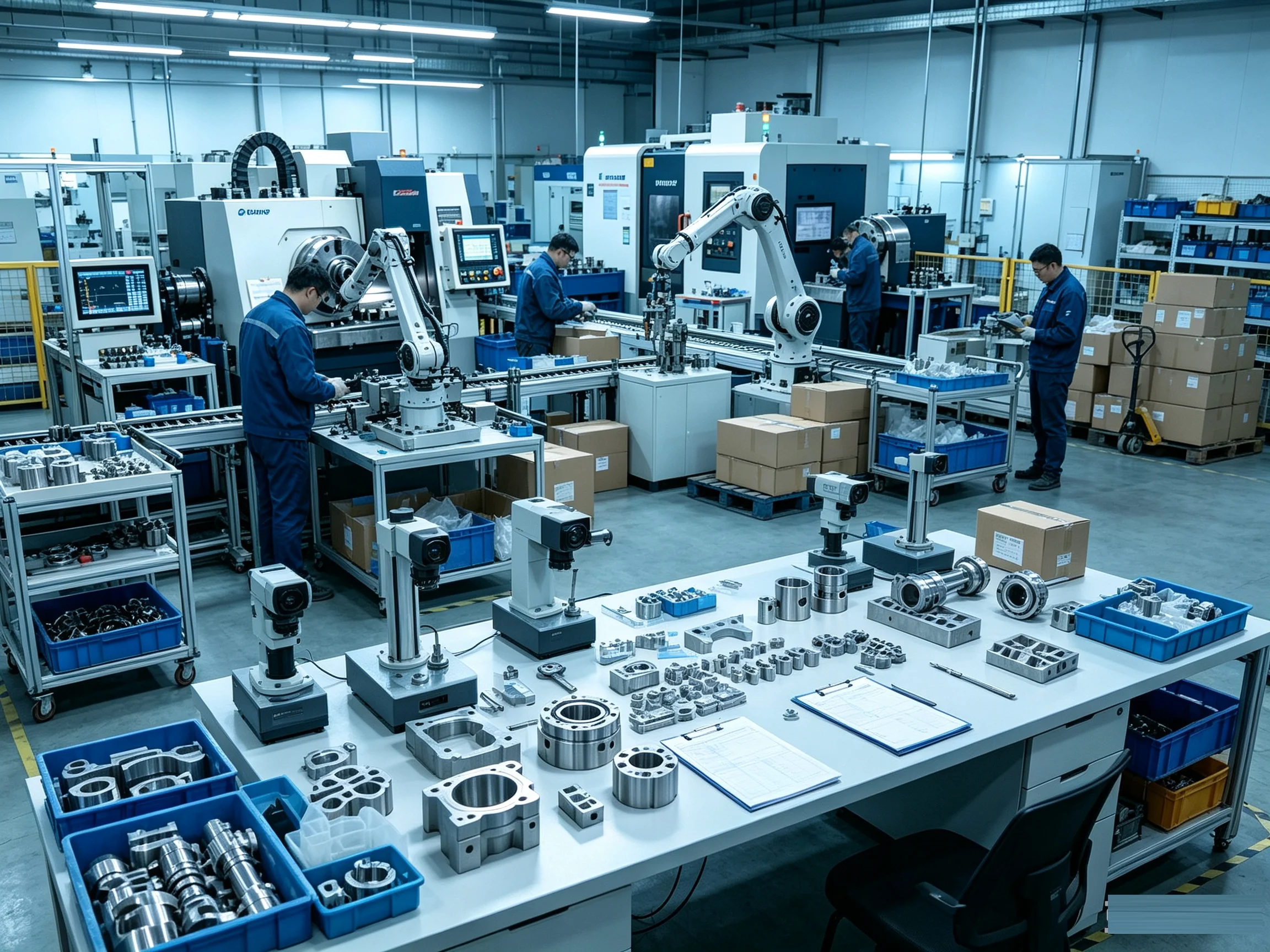
Our Factorys
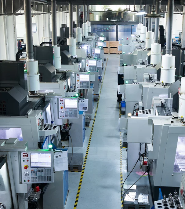
CNC Machine Shop
Established:2015
Number of Machines:500 Machines
Location:ShenZhen
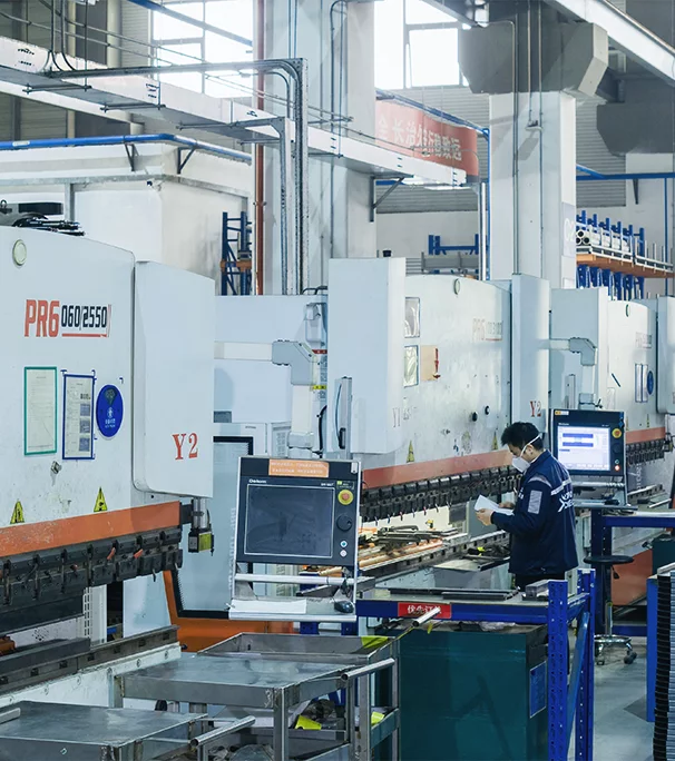
Sheet Metal Factory
Established:2019
Number of Machines:150 Machines
Location:ShenZhen
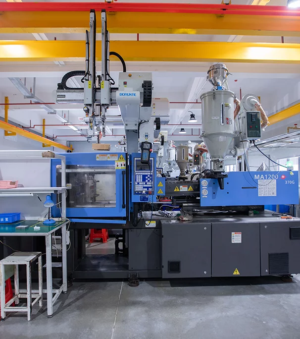
Jnjection Molding Factory
Established:2018
Number of Machines:350 Machines
Location:FoShan
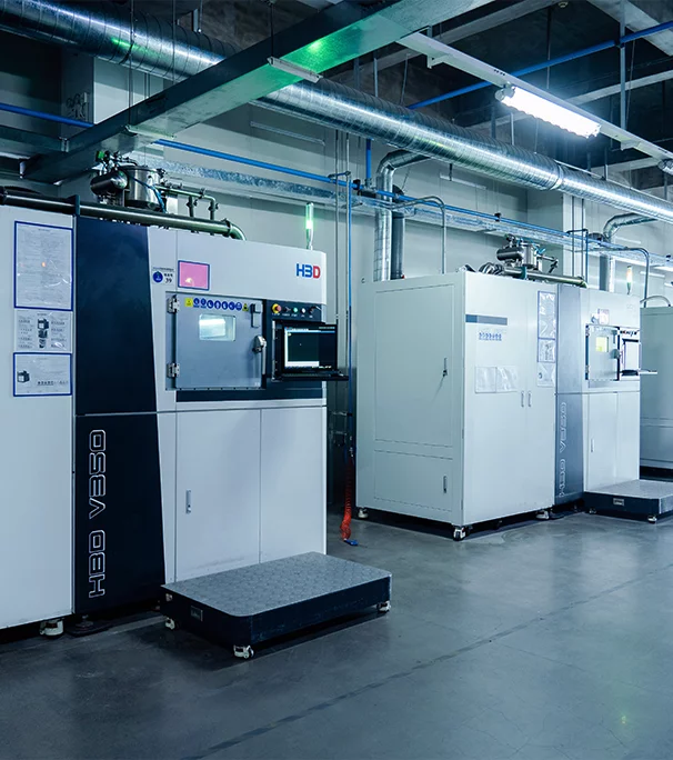
3D Printing Factory
Established:2015
Number of Machines:300 Machines
Location:ShenZhen
Vacuum Casting Factory
Established:2013
Number of Machines:220 Machines
Location:DongGuan
Die Casting Factory
Established:2017
Number of Machines:100 Machines
Location:ShenZhen
SUDACNC Trusted Global Partner
We are your trusted manufacturing partner. Precision Machining and Efficient Management Delivery of High-Accuracy Global Parts. We guarantee consistent quality and transparency with punctual and reliable lead times.
We are with you every step of the way, from validating a design to mass production.
30M+
Network-wide parts produced
5,000+
Companies served
5,200+
Combinations of material, process, finish
options
30+
Supply regions to mitigat e risk & enhance delivery speed
Metal and Plastic Production Solutions
SUDACNC’s digital manufacturing marketplace is your one-stop solution for production. Our team is the perfect solution for your product manufacturing needs with our staff of technical experts, ease of our secure quoting platform, and global manufacturing capacity.
SUDACNC offers competitive pricing and lead times on plastic injection molding, die casting, metal stamping, metal extrusion, plastic extrusion, sheet metal, laser cutting, waterjet cutting, laser tube cutting, and tube bending services. Start your quote or contact us today to begin.
Choose Your Optimal Price and Lead Time
The SUDACNC Instant Quoting Engine® makes it easy to upload a CAD file and compare prices and lead times in just a few clicks. With thousands of manufacturing suppliers in all 50 U.S. states and more than 20 countries, SUDACNC’s extensive network gives you options to choose the shipping timeline and price that fit your business and budget.
SUDACNC offers price matching and a 30-day price guarantee on quotes, giving you peace of mind that you’re getting the best price. When ordering prototypes — originals or models of parts that are intended exclusively for non-commercial purposes — the price shown at checkout includes tariffs. Shipping is also included, as long as your package is standard-size.
Our Works
Our Works-area
Our Works 2
Our Works 3
Our Works 4
Our Works 5
Our Works 6
Our Works 7
Our Works 8
Our Works 9
Our Works 10
Our Works 11
Our Works 12
Our Works 13
SUDACNC Four Workflow Phases
From start to finish, our process is built for speed and clarity. Each step is transparent, keeping you in control. The result: precision results delivered on time.
Real-Time Quotes
Confirm transparent price structures, timelines, and DFM visibility in minutes, with the SUDACNC quoting engine supporting optimal strategic decisions. Upload your CAD files to reduce time spent in quoting cycles.
Quality Assurance
SUDACNC enables you to access a single, streamlined platform for managing versatile professional collaborative relationships with certified suppliers and diverse manufacturing capabilities, allowing you to scale production to meet unlimited volume requirements.
Deep Manufacturing Network
Every part of SUDACNC goes through rigorous inspection standards to ensure that we meet all your dimensional, cosmetic, and performance needs and requirements.
Industry-Focused Expertise
SUDACNC works across multiple industries, including aerospace, automotive, medical, robotics, consumer, and industrial machinery, delivering consistent quality in highly demanding projects.
All-in-One Your Reliable Manufacturing Partner
Design&Engineering Support
Rapid Prototyping
Production and Manufacturing
Quality control and distribution
Design and Engineering Support
Our work begins with understanding your design with engineering clarity. Knowing that the starting point of every successful product is understanding the engineering aspect, we work with you to comprehend design needs, analyze the specifications, and make manufacturable parts. Our early risk assessments streamline revisions, contain costs, and deal with ever-decreasing performance variability.
Practical DFM Comments to Support Design Decision Improvementss
Material Suggestions Based on Your Application
Engineering Assistance to Boost Efficiency and Longevity
Rapid Prototyping
Change concepts into real-life components fast and with ease. Rapid Precision services enable you to validate your design, test its functionality, and work out any remaining details before entering the production phase, allowing complete design confidence. Directly accompanying any design stage, fast production welcomes you to the design stage without demand to sacrifice precision.
Quick prototypes to perform experiments.
Prototypes for Form, Fit, and Function Validation
Prototyping is Perfect for Design Validation, Demonstration, and Initial Production Stages.
Production and Manufacturing
When your design is production-ready, we make the transition to production seamlessly. Supporting low, medium, and high-scale production, we maintain the same quality, repetition, and precision in each manufacturing run. Adaptable workflows allow for smooth production transitions as demand increases.
Encompassing all aspects of manufacturing
Consistency and repeatability across all ranges of production
Versatile manufacturing capabilities
Quality control and distribution
The meticulous nature of our work carries through all aspects of our business. Each component undergoes a thorough review to meet the required specifications and standards to be qualified for shipping. Following our extensive and streamlined order delivery process, we guarantee our customers receive parts that are ready to be joined and utilized for intended purpose in a timely fashion, without exception.
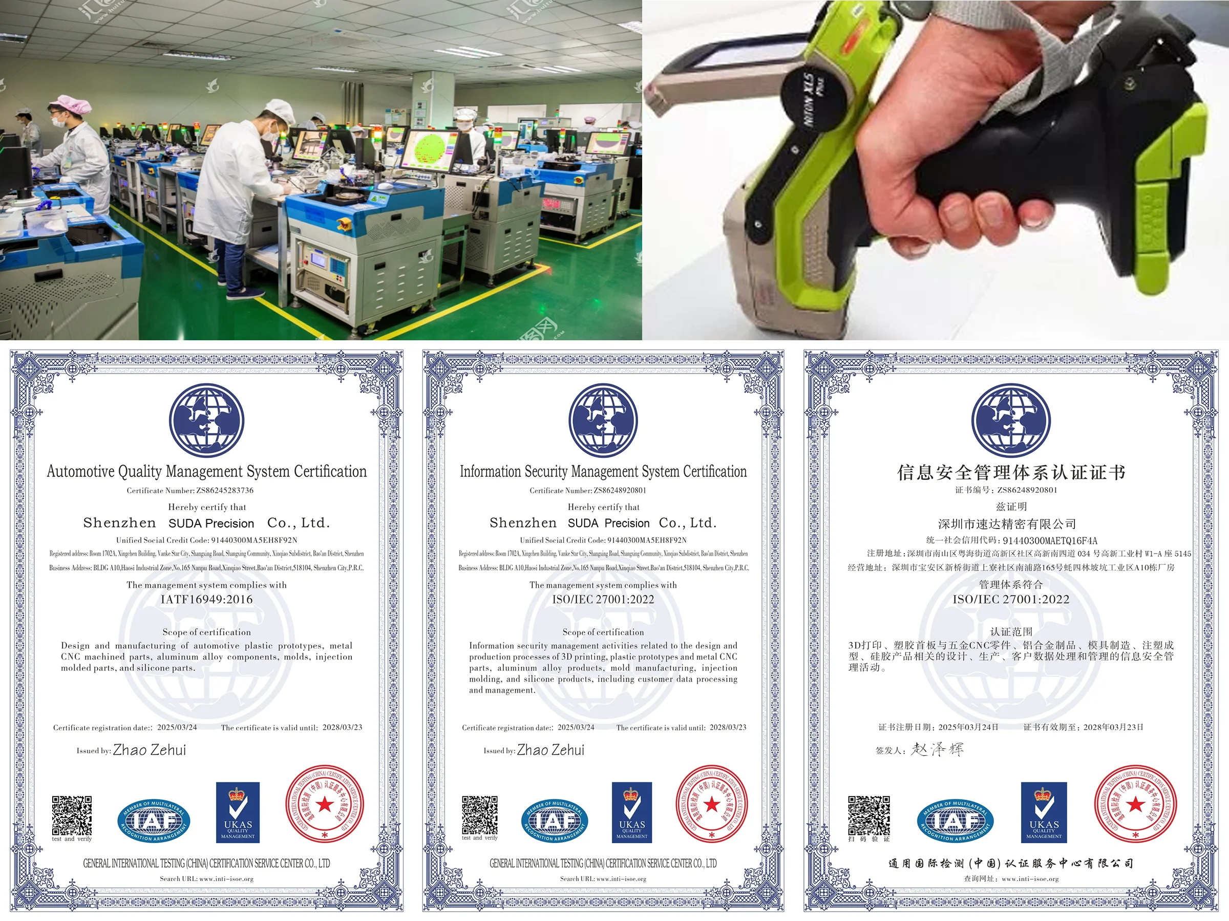
Quality control aligned with ISO standards
Quality documentation with complete traceability
Accurate delivery to all parts of the world
Quality Assurance & Compliance
in Every Part We Manufacture
We stay true to industry standards that have to do with quality and safety, like ISO 9001:2015 and AS9100. We assess and check every part multiple times to ensure that inspections have been done thoroughly and that we can offer no exceptions to your needs.
ISO 9001 Certified
100% Quality Inspection
Premium Material Selection
What Makes SUDACNC Different from Others
Instant Smart Quoting
Get quick pricing and DFM insights to optimize designs and reduce costs.
Global Supply Network
Access our global manufacturing network for reliable solutions of all sizes.
Certified Quality Control
Strict inspection protocols for every part. We ensure 100% accuracy and high standards.
Fast Reliable Delivery
Punctual shipping for all custom orders. Your projects always stay on schedule.
Our rich project experience accumulation and pre-analysis before production enable us to consider comprehensively and provide the mostsuitable and economical solutions, to
ISO 9001 Certified
100% Quality Inspection
Premium Material Selection
Save Your Time
Our skilled engineers team and sales
team work close to make professionaland efficient communication with thecustomers, to save the time.
48-Hour Standard Delivery
Express 24-Hour Option
Real-Time Order Tracking
Responsible and efficient after-salesservice
We will absolutely take our responsiblityfor any potential part quality issue, andcommunicate and solve it timely to meetcustomer's demand.
Expert Technical Consultation
Custom Solution Development
Dedicated Support Specialists
What Our Clients Say
"Implementing their precision-engineered components has dramatically lowered our operational overhead. The technical support team provided exceptional guidance in tailoring the ideal setup for our specialized manufacturing floor."
— Emily Watson, Head of Manufacturing
"Faced with a sudden shortage on our main assembly line, their team expedited the critical components within a day, preventing catastrophic financial losses. Their agility and customer-first mindset make them a premier strategic partner."
— David Lin, Supply Chain Director
"The dimensional consistency of their CNC parts is flawless, which seamlessly integrated into our rigid Outgoing Quality Control protocol. We haven't had a single batch rejection since switching to their fulfillment services."
— Marcus Vance, Quality Assurance Manager
"Their end-to-end transparency and automated dispatch tracking have revolutionized how we manage our warehouse flow. It's rare to find a manufacturing vendor that pairs heavy industrial expertise with such agile digital efficiency."
— Sophia Zheng, Procurement Specialist
Ready to Experience the Difference?
Join hundreds of satisfied customers who trust us for quality, speed, and expertise.