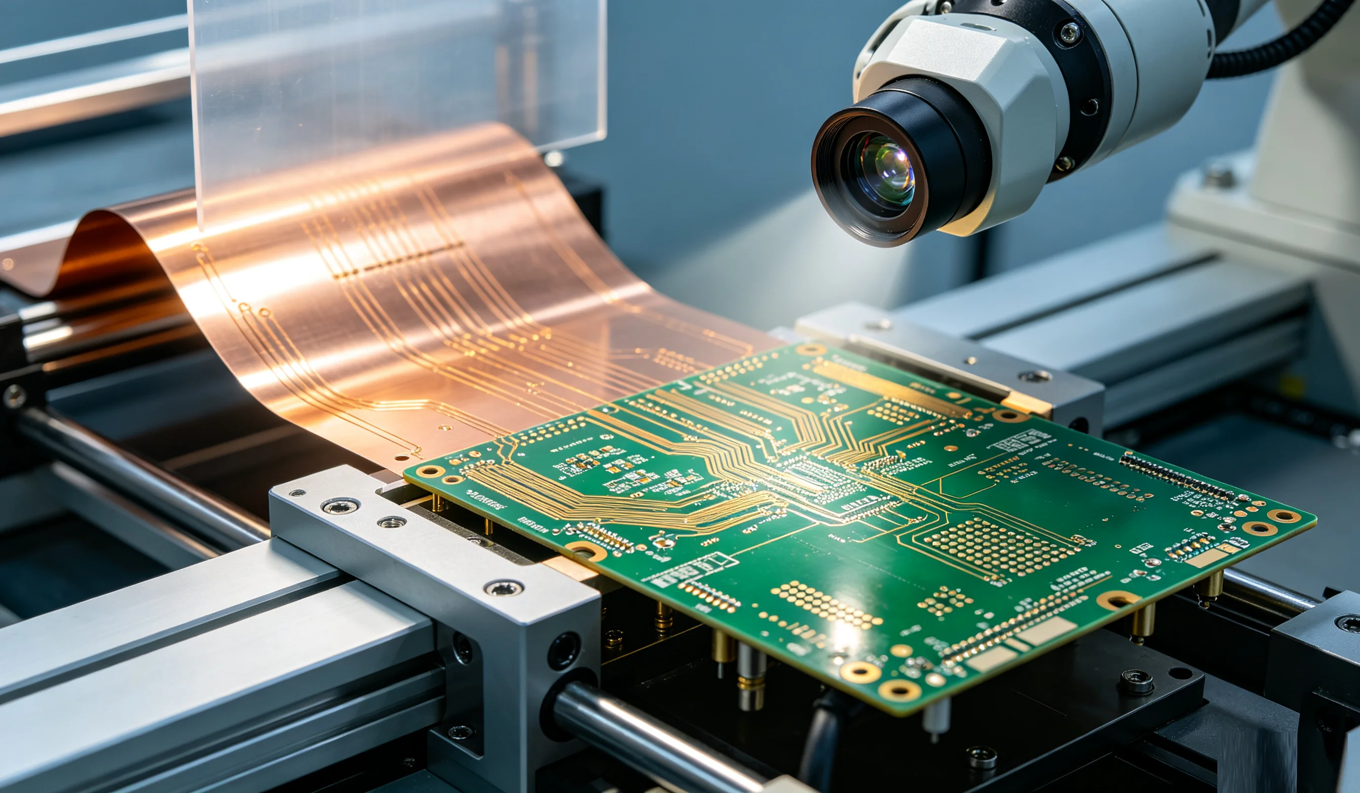
SUDACNC operates full in-house PCB bare board manufacturing production lines to deliver high-precision custom circuit board fabrication for global OEM & ODM electronics developers. Our complete fabrication workflow includes DFM manufacturability review, layer lamination, laser & mechanical drilling, copper plating, impedance matching, solder mask printing, surface finishing and 100% electrical testing. We manufacture all mainstream PCB variants: multi-layer rigid FR4, halogen-free high Tg board, flexible FPC, rigid-flex composite, HDI blind/buried microvia, aluminum metal core MCPCB for power LED drivers, and high-frequency RF PCB with Rogers/Taconic substrates. Strictly follow IPC-6012/6013 workmanship standards, certified UL, RoHS, ISO9001, IATF16949 automotive and ISO13485 medical compliance. We support independent bare PCB supply and full turnkey design + fabrication + PCBA assembly closed-loop service, directly docking our internal PCB design and SMT/THT assembly workshops to eliminate cross-supplier communication errors and shorten hardware development cycles.
Request PCB Manufacturing Quotation
Gerber, Drill, Stack-Up Spec, Datasheet & Material Requirements Accepted
All design files protected under formal NDA confidentiality agreement
Full in-house production without outsourcing third-party factories
What Is PCB Manufacturing (PCB Fabrication)?
PCB Manufacturing, also known as PCB Fabrication, is the complete industrial process to convert PCB layout Gerber files into physical bare printed circuit boards without soldered components. It covers core processes including inner layer circuit imaging, multi-layer hot press lamination, precision drilling, hole copper plating, outer layer etching, solder mask protection, silkscreen legend printing, surface finish treatment and final electrical continuity testing.
Many electronics brands outsource PCB production to external third-party fabs, which easily cause mismatched process parameters with subsequent PCBA assembly lines. Our integrated factory owns independent PCB manufacturing plant matched with our own SMT cleanroom assembly standards, DFM engineers fully familiar with internal production limits, effectively reduce prototype rework rate. We support small rapid prototype batches and large mass volume production, covering consumer IoT, industrial control, automotive, medical and wireless communication hardware circuit board demands.
Six Closed-Loop Full-Process PCB Fabrication Modules
Our PCB manufacturing adopts standardized six-step closed-loop production workflow, covering pre-production engineering validation, core circuit fabrication, drilling & plating, surface finishing, full quality testing and final packaging shipment. All production processes follow IPC international standards, each batch recorded for full traceability. We support two independent cooperation modes: independent bare PCB supply (customer self-arrange subsequent PCBA assembly) and full turnkey PCB design + fabrication + SMT/THT assembly one-stop hardware development, eliminating multi-supplier coordination troubles for electronic brand customers.
Unique Strengths Of Our Self-Owned PCB Fabrication Factory
Full In-House Independent Production: No external outsourcing, all processes lamination, drilling, plating, testing completed in our own workshop, stable quality control
Full PCB Type Integrated Production: Rigid/FPC/Rigid-Flex/HDI/MCPCB/RF high-frequency single factory full coverage, no split order to different fabs
Professional Impedance Stack-Up Calculation Team: Custom stack-up report for high-speed differential signal & RF antenna PCB, accurate impedance matching
Submit Gerber, Stack-Up & Material Spec For Free PCB DFM Review & Fabrication Quotation
Six Main Categories Of Custom PCB We Produce In-House
We adjust stack-up, substrate material, copper weight and drilling process according to different PCB types and application scenarios, fully matching the electrical and mechanical reliability requirements of each industry product.
1~32 layer FR4 glass fiber rigid circuit board, optional high Tg, halogen-free substrate, low cost and stable mechanical performance. Suitable for consumer electronics, industrial control, IoT sensor mainboards, automotive low-speed control modules. Support general digital circuit, power circuit, medium-speed signal layout, customizable heavy copper 2oz/3oz/4oz high-current power supply board fabrication.
Polyimide PI ultra-thin flexible substrate, reserved smooth bending arc, anti-crack trace design, minimum 0.1mm board thickness. Rigid-flex combines rigid FR4 functional zones and flexible bending zones integrated into one panel, eliminate connector wiring. Widely applied in wearable medical devices, smart watch internal connection boards, foldable consumer electronics, portable detection equipment.
Adopt sequential lamination, laser blind & buried microvia stacking technology, greatly improve wiring density, support 0201 miniature components and 0.4mm ultra-fine pitch BGA/QFN chips. Ideal for compact handheld devices, portable medical sensors, mini IoT control modules with limited enclosure space, realize smaller PCB size and thinner overall thickness.
Aluminum base PCB as mainstream type, ultra-high thermal conductivity substrate, fast heat dissipation for high-power LED lighting, motor drive power modules, automotive headlight driver boards. Copper base MCPCB for ultra-high power heat dissipation scenarios, insulation dielectric layer thickness customizable, support heavy copper traces for large current transmission, effectively reduce chip operating temperature and extend service life.
Special low Dk/Df high-frequency dielectric substrates, precise 50Ω single-ended / 100Ω differential impedance control, stable signal transmission at high frequency bands from Sub-GHz to 5G mmWave. For wireless communication modules, remote control, Bluetooth/WiFi gateway, radar antenna circuit boards, minimize signal attenuation and interference during high-frequency signal transmission.
Automotive PCB adopt high Tg low warpage FR4 material, wide temperature range stack-up design, anti-vibration copper layout, comply with AEC-Q100 supporting production rules. Medical PCB use low-noise low ion migration substrate, strict impurity control, full batch material traceability, match ISO13485 cleanroom assembly manufacturing requirements, suitable for vital sign monitoring and diagnostic equipment circuit boards.
Custom PCB Substrate, Layer Count & Special Process Fabrication Solution
Uniform flat surface, excellent oxidation resistance, long storage life, compatible with SMT fine pitch BGA/QFN soldering, good wire bonding performance. Most widely used surface finish for industrial control, medical, automotive, high-reliability IoT PCBs, premium general-purpose surface treatment with stable assembly yield.
Low cost, flat copper surface, no nickel barrier layer affecting high-frequency signal loss, ideal for high-speed digital and RF wireless PCB. Short storage cycle, sensitive to repeated high-temperature reflow, suitable for consumer electronics prototype and mass production boards with short assembly cycle.
Most economical surface finish, thick solder layer good for THT through-hole soldering, easy rework and repair. Slightly uneven tin surface not suitable for ultra-fine pitch 0.4mm BGA chips, widely used for low-speed power supply, simple consumer double-layer PCB mass production.
Immersion Silver: Ultra-flat surface, good high-frequency performance, suitable for RF antenna PCB, short shelf life needs sealed packaging. Immersion Tin: Good solderability, low cost alternative to ENIG, easy oxidation requiring short-term assembly, used for medium-volume industrial control circuit boards.
Thick hard gold plating on connector edge fingers, wear-resistant for repeated plug-in cycles, anti-corrosion for long-term storage. Custom selective gold plating only on contact areas to save cost, applied to memory card PCB, industrial communication interface board, charging connector circuit boards.
Custom Surface Finish Selection Advice Based On Your Assembly & Storage Requirements
Critical IPC DFM Design For Manufacturing Mandatory Rules
PCB Layout DFM Feature
Manufacturing Process Limit Rule
Minimum Trace Width / Spacing (Standard FR4)
≥0.10mm / 0.10mm; HDI micro line ≥0.075mm / 0.075mm
Minimum Mechanical Drill Hole Diameter
≥0.15mm finished hole; laser microvia ≥0.10mm
Minimum Annular Ring Around Holes
≥0.06mm to prevent copper ring breakage during drilling
Solder Mask Bridge Minimum Width
≥0.04mm to avoid mask bridging short circuit during exposure
PCB Edge Keep-Out Clearance
≥3mm reserved margin for SMT conveyor fixture clamping
Copper To Board Edge Clearance
≥0.2mm prevent copper exposure after CNC routing
HDI Microvia Stacking Aspect Ratio
Max 15:1 comply with IPC lamination & plating standard
Free Pre-Production Full DFM Review Before PCB Mass Fabrication
Core Industry PCB Fabrication Application Scenarios
Automotive Electronics PCB Fabrication
BMS battery management multi-layer PCB, vehicle sensor control boards, car lighting aluminum MCPCB, infotainment high-speed communication boards, high Tg low warpage substrate, wide temperature resistant stack-up, IATF16949 certified production process, full batch material traceability management.
Medical Device PCB Fabrication
Wearable vital sign FPC flexible board, diagnostic equipment multi-layer HDI PCB, low noise analog signal circuit boards, low ion migration substrate, strict impurity control, ISO13485 compliant manufacturing, full raw material batch record archive for audit inspection.
Industrial Control & IoT Hardware PCB
PLC main control multi-layer PCB, industrial gateway high-speed differential signal board, wireless RF antenna PCB, power drive aluminum base MCPCB, heavy copper power traces, optional thick ENIG surface finish for long-term harsh factory environment stable operation.
Consumer & Communication Electronics PCB
Smart home controller 2/4 layer rigid PCB, wearable watch mini HDI board, Bluetooth audio circuit board, 5G small signal Rogers RF PCB, cost optimized OSP/HASL surface finish for mass volume standardized consumer hardware production.
Custom PCB Fabrication Engineering Solutions For Your Industry Electronic Hardware Projects
Mandatory production files: Gerber RS274X copper/solder mask/silkscreen layers, NC drill file, PCB outline drawing; auxiliary documents: layer stack-up specification, impedance requirement, material datasheet, surface finish demand, special process instructions.
No strict MOQ limit, support flexible order volume: 1–10pcs rapid prototype samples (3–5 working days fast turnaround), small batch 50–500pcs, medium volume 1,000–50,000pcs, large mass production over 100,000pcs, independent prototype dedicated production line to avoid mass production scheduling delays.
Two independent cooperation modes available: 1. Independent bare PCB manufacturing only, deliver finished bare boards for customers to arrange third-party SMT assembly; 2. Full turnkey PCB design + fabrication + PCB Assembly PCBA one-stop closed-loop manufacturing, unified schedule and quality control with shorter overall hardware development cycle.
Simple 2-layer FR4 prototype PCB: 3–5 working days; standard 4–6 layer rigid PCB small batch: 5–8 days; HDI / FPC / aluminum MCPCB medium batch: 8–12 days; high-frequency Rogers multi-layer automotive/medical high-reliability PCB: 12–20 working days including full impedance testing and inspection.
ISO9001 quality management system, UL PCB safety certification, RoHS & halogen-free environmental compliance, IATF16949 automotive electronics manufacturing certification, ISO13485 medical device production system, fully comply with IPC-6012 / IPC-6013 international PCB fabrication workmanship standards.
Independent Bare PCB Fabrication VS Full Turnkey Design+Fab+PCBA Service Comparison Table
Swipe horizontally to view full table columns
Comparison Item
Independent Bare PCB Manufacturing Only
Full Turnkey PCB Design + Fabrication + PCBA Assembly
Deliverable Scope
Only finished bare PCB panels with surface finish & electrical test report, no component assembly service